Mastering PCB Printing: A Comprehensive Guide on How to Print PCB
Printing Printed Circuit Boards (PCBs) is a fundamental aspect of electronics manufacturing. Whether you’re a hobbyist or a professional, mastering PCB printing techniques is crucial for creating functional and reliable electronic devices. In this comprehensive guide, we’ll delve into the step-by-step process of printing PCBs, from design to production, covering essential tips, techniques, and best practices along the way.
Understanding PCB Printing

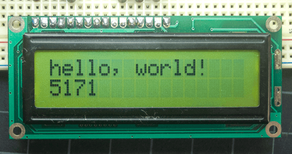
Before diving into the printing process, let’s briefly understand what PCB printing entails. PCB printing involves transferring a designed circuit layout onto a board using specialized techniques. This process creates the conductive pathways that connect electronic components, forming the backbone of electronic devices.
Steps on how to print Printed Circuit Board
These are the steps on how to print your printed circuit boards:
Step 1: Designing the PCB
The first step in PCB printing is designing the circuit layout using PCB design software such as Altium Designer, Eagle, or KiCad. During this phase, you define the components, trace routing, and signal paths of your circuit. Pay attention to factors like component placement, trace thickness, and spacing for optimal performance.
Step 2: Generating Gerber Files
Once the design is complete, generate Gerber files from your PCB design software. Gerber files contain the necessary information for PCB fabrication, including copper layers, solder mask, silkscreen, and drill files. Ensure compatibility with your chosen PCB manufacturing process and specifications.
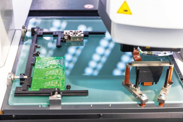
Step 3: Choosing the Printing Method
There are several PCB printing methods available, including:
- Etching: Traditional method involving chemical etching of copper-clad boards to remove unwanted copper.
- Direct Ink Printing: Using specialized inkjet printers to print conductive ink directly onto the substrate.
- Laser Printing: Using lasers to selectively remove copper from coated substrates, creating the circuit pattern.
- DIY Methods: Including toner transfer, CNC milling, or 3D printing for prototyping purposes.
Choose the method that best suits your budget, equipment availability, and desired PCB complexity.
Step 4: Printing the PCB

Depending on your chosen method, follow these general steps:
- Etching: Print the circuit design onto transfer paper, transfer it onto the copper-clad board, and etch using a suitable etchant solution.
- Direct Ink Printing: Load conductive ink into the inkjet printer, print the circuit design directly onto the substrate, and cure according to manufacturer instructions.
- Laser Printing: Use a laser engraving machine to remove copper from the substrate based on the circuit design, then clean and inspect the board.
- DIY Methods: Follow specific instructions for toner transfer, CNC milling, or 3D printing, ensuring accuracy and alignment with the Gerber files.
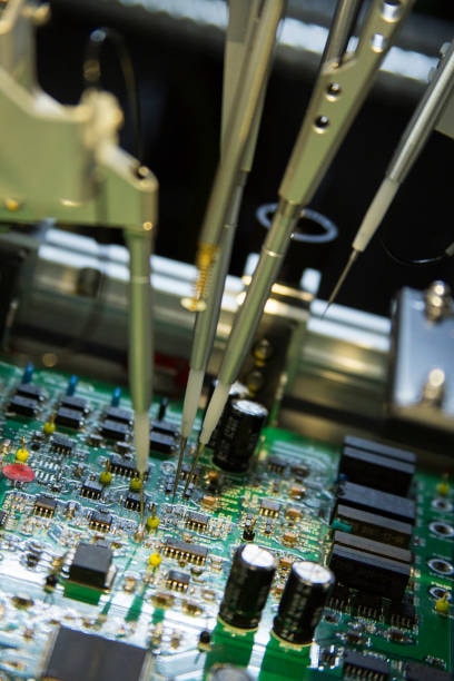
Step 5: Post-Printing Processes
After printing, perform post-printing processes to enhance PCB functionality and durability:
- Solder Mask Application: Apply solder mask to protect traces and pads, improve solderability, and prevent shorts.
- Silkscreen Printing: Add component labels, logos, and reference marks using silkscreen printing for easier assembly and troubleshooting.
- Drilling: Drill holes for component mounting and vias using a PCB drill machine, aligning with drill files from the Gerber data.
- Surface Finish: Apply surface finish (e.g., HASL, ENIG, OSP) for protection against oxidation and to facilitate soldering during assembly.
Frequently Asked Questions
What is PCB printing, and why is it important?
A1: PCB printing refers to the process of transferring a designed circuit layout onto a board using specialized techniques. It’s important because PCBs form the foundation of electronic devices, providing the necessary conductive pathways for components to function.
What software is used for designing PCBs?
A2: Popular PCB design software includes Altium Designer, Eagle, KiCad, and OrCAD. These tools allow engineers to create circuit layouts, define components, and optimize trace routing for efficient PCB production.
What are Gerber files, and why are they essential for PCB printing?
A3: Gerber files contain the information needed for PCB fabrication, including copper layers, solder mask, silkscreen, and drill files. They are essential because PCB manufacturers use Gerber files to accurately reproduce the circuit design during production.
What are the different methods of PCB printing?
A4: PCB printing methods include etching, direct ink printing, laser printing, and DIY methods like toner transfer or CNC milling. Each method has its advantages and is chosen based on factors such as complexity, budget, and equipment availability.
How does the etching method work for PCB printing?
A5: In the etching method, the circuit design is printed onto transfer paper and then transferred onto a copper-clad board. The board is then etched using a chemical solution that removes unwanted copper, leaving behind the desired circuit pattern.
What is direct ink printing, and what are its benefits?
A6: Direct ink printing involves using specialized inkjet printers to print conductive ink directly onto the substrate, creating the circuit pattern. It offers benefits such as rapid prototyping, precise trace alignment, and the ability to print complex designs.
Can PCBs be printed using laser technology?
A7: Yes, laser printing is a viable method for PCB production. Laser engraving machines selectively remove copper from coated substrates based on the circuit design, offering high precision and accuracy in creating intricate circuit patterns.
What are the post-printing processes involved in PCB production?
A8: Post-printing processes include applying solder mask for protection, silkscreen printing for labeling and reference marks, drilling holes for component mounting and vias, and applying surface finish for oxidation protection and solderability.
How can beginners start learning PCB printing?
A9: Beginners can start by learning PCB design basics using software tutorials and online resources. They can then experiment with simple PCB printing methods like toner transfer or direct ink printing to gain hands-on experience.
What are some common challenges in PCB printing, and how can they be overcome?
A10: Common challenges include alignment errors, trace thickness inconsistencies, and solder mask defects. These challenges can be overcome by using accurate printing techniques, optimizing design layouts, and conducting thorough quality checks during production.
Conclusion
In conclusion, mastering PCB printing is a journey that blends creativity, precision, and technical expertise. This comprehensive guide has provided a roadmap from PCB design to production, covering essential steps such as designing the circuit layout, generating Gerber files, choosing the printing method, executing the printing process, and conducting post-printing processes. By following these steps and leveraging the right tools and techniques, individuals can create high-quality PCBs that meet industry standards and fulfill the requirements of various electronic applications.
As technology continues to evolve, PCB printing techniques and tools will also advance, offering new possibilities and innovations in electronics manufacturing. It’s essential for PCB enthusiasts, hobbyists, and professionals to stay updated with industry trends, explore emerging printing methods, and continuously refine their skills to excel in the dynamic field of PCB printing. With dedication, practice, and a passion for electronics, anyone can master PCB printing and contribute to the development of innovative electronic devices that shape the future.
Summary
Mastering PCB printing requires a combination of meticulous design, technical knowledge, and practical skills. This guide has outlined the fundamental steps involved, from designing the circuit layout and generating Gerber files to choosing the appropriate printing method and conducting post-printing processes. Understanding the importance of each stage and adhering to best practices ensures the creation of high-quality PCBs that meet industry standards and functional requirements.
Moreover, as technology advances, new printing methods and materials emerge, offering opportunities for innovation and efficiency in PCB production. Staying informed about these developments, experimenting with different techniques, and continuously honing one’s skills are key to mastering PCB printing and staying at the forefront of electronics manufacturing. With dedication and a commitment to excellence, individuals can unlock the full potential of PCB printing and contribute to the advancement of electronic devices across various industries.